기술 소개
공정 장비 활용
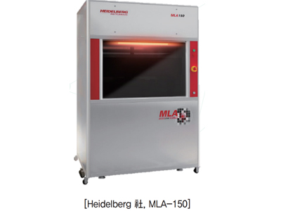
01 Direct Writing Lithography 기술 (Laser Lithography)
Equipment
- Optical system: highly reflective mirrors and DMD™ (down to 1 μm feature size)
- Stage System
- Substrate size: 5×5 mm² ~ 8-inch wafer
- Maximum write area: 200 × 200 mm²
- Interferometer resolution: 20 nm
- Diode Laser Illumination Module: 405 nm / 8 W
- Autofocus System: Real-time air-gauge autofocus (dynamic range: 80 μm)
Applications
- Backside alignment
- Global & field-by-field alignment
- Fast, high-precision alignment
- Alignment accuracy < 500 nmProcess Result
Process Result

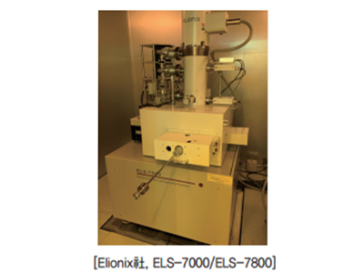
02 Direct Writing Lithography 기술 (E-Beam Lithography)
Equipment
- Acceleration voltage: ~100 keV
- Wafer size: piece to 200 mm
- Field size: 600 μm × 600 μm (Max)
- Minimum line width: 10 nm
- Alignment accuracy: 25 nm
- Beam current: 1×10⁻¹² ~ 2×10⁻⁹ A
- Beam shape: Gaussian
- Data formats: *.sch, *.con, *.ccc, *.cbc, *.cel
Applications
-
Applicable to a wide range of nanostructured devices, including electronic devices, optoelectronic devices, quantum
structures, metamaterials, semiconductor–superconductorinterface studies, MEMS, optical and photonic devices. - Also suitable for mask fabrication and direct writing on non-planar substrates
Process Result


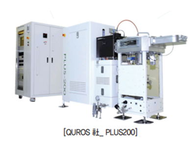
03 High-k 증착 기술 (ALD)
Equipment
- Wafer size: up to 8-inch wafer
- Base pressure: ≤ 10 mTorr (PM 기준)
- Process temperature range: up to 650 ℃
- RF plasma power: 1,000 W (13.56 MHz)
- Precursors: TMA, TEMAHf, TEMATi
- Process gases: O₂, NH₃, Ar, N₂
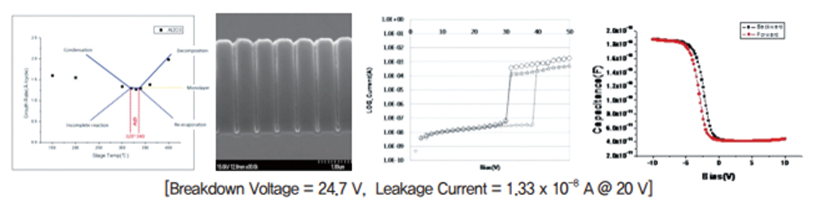
ALD Process Performance
- Deposition: Al₂O₃, HfO₂ (PM1), TiN (PM2)
- Thickness uniformity: < 1.5% (1 sigma)
- Step coverage: > 95%
Applications
- High-k gate oxides for SiC·GaN power MOSFET integration, increasingly adopted in recent studies
Process Result
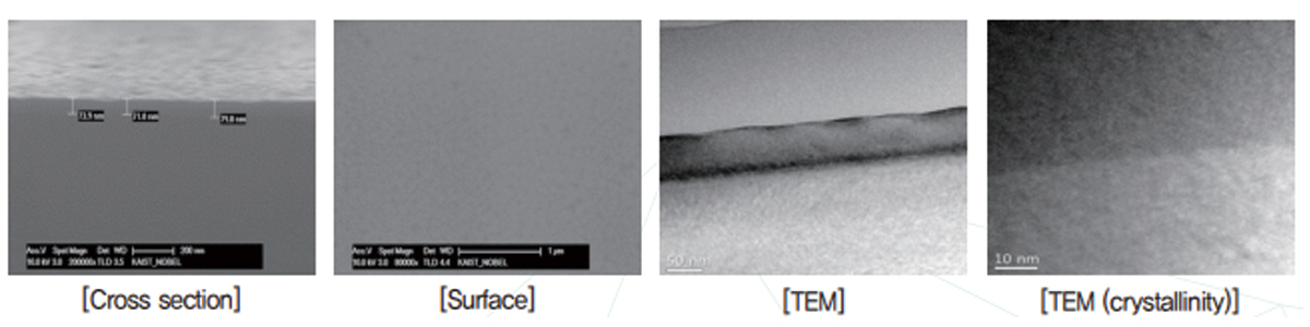
04 Epi 성장 기술 (UHV-CVD)
Equipment
- Wafer size: up to 8-inch wafer
- Base pressure: < 5 × 10⁻⁹ Torr
- Process temperature: 300–750 ℃
- RF plasma power: 600 W (13.56 MHz)
- Process gases: Si₂H₆, GeH₄, CH₃SiH₃, 0.5% B₂H₆/He, 0.5% PH₃/He
SiGe Process Performance
- Selective SiGe epitaxy on Si substrate
- Uniform Ge concentration
- Thickness uniformity: < 3.0% (1 sigma)
- Growth rate & Ge-content control via GeH₄ flow
Applications
- IBM demonstrated the world’s fastest SiGe-based semiconductor circuit, operating at over 110 GHz and capable of
processing electrical signals in just 4.3 trillionths of a second.
Process Result
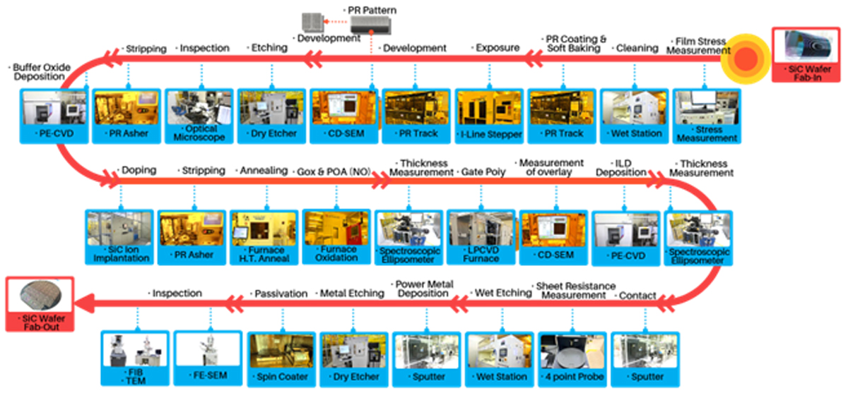
05 SiC·GaN 전력소자 제작 기술
Equipment
- Photo: I-Line Stepper(i10C), PR Track(Mark-7), Aligner(MA6)
- Cleaning & Etching: Wet station, Dry Etcher_20 nm, ICP-RIE
- Thin Film & Diffusion: Furnace, Implanter, LP-CVD, ALD
- RF plasma power: 600 W (13.56 MHz)
- Inspection: CD-SEM, FE-SEM, OP3260, 4PP, 3D Profiler, Stress Measurement
Applications
- 초고전압 분야에서 신뢰성·제어성·효율성 향상
- 시스템 소형화 및 에너지 절감
- 열방열 분야의 소형화 및 비용 절감
- 자동차 및 산업용 전력변환 시스템(Converter, Inverter 등)
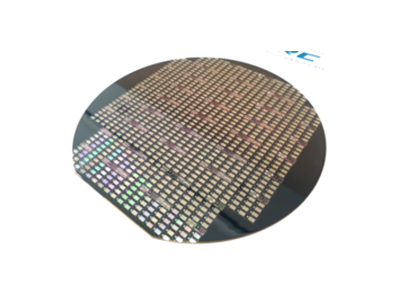
Fabrication Result
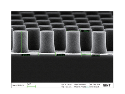
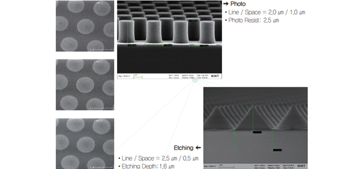
06 Patterned Sapphire Substrate (PSS) 제작 기술
Equipment
- Photo: Stepper ≥ 0.4 μm (5:1 Reticle Lithography)
- Cleaning & Etching: Wet station, ICP Dry Etcher
- Inspection: CD-SEM, FE-SEM, 3D Profiler
Applications
- LED Sapphire 기판 렌즈 패턴 형성
- 난반사 제어 기반 광출력 향상
- Dot patterning 및 Sapphire·PR 선택적 식각 기반 depth control
- 자동차 및 산업용 전력변환 시스템(Converter, Inverter 등)
Fabrication Result
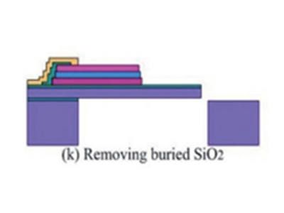
07 Micro Cantilever 제작 기술
Equipment
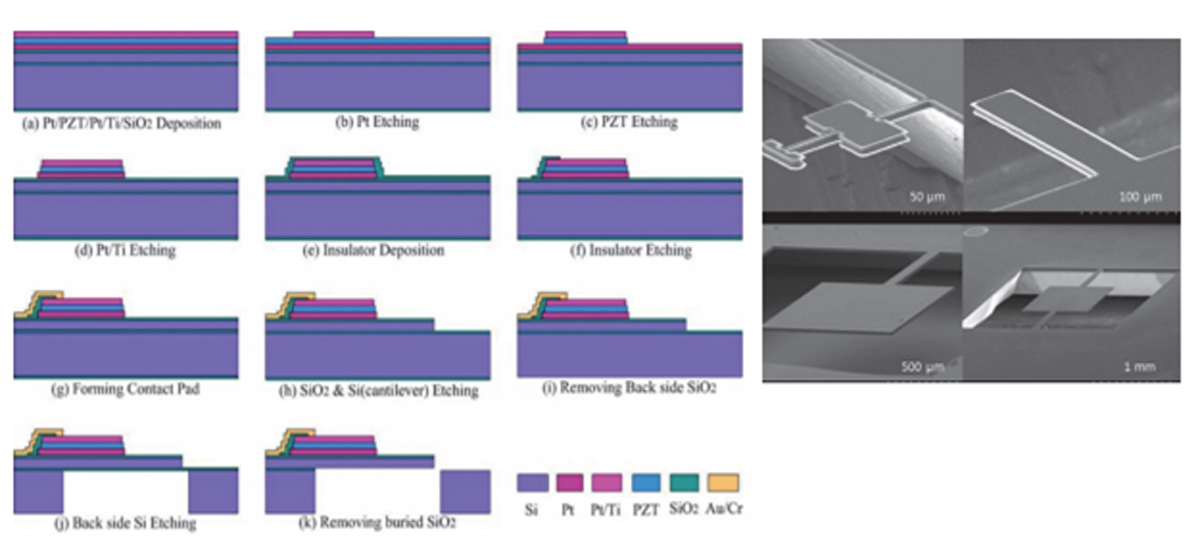
- Photo: Aligner(MA6), Laser Lithography
- Cleaning & Etching: Wet station, Dry Etcher_20 nm, ICP-RIE, DRIE
- Thin Film & Diffusion: E-Beam Evaporator, LP-CVD, PE-CVD
- Inspection: CD-SEM, FE-SEM, 3D Profiler
Applications
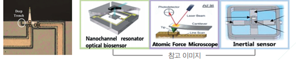
- 압전 트랜스듀서, 캔틸레버·멤브레인 센서
- SPM Probe, 마이크로폰
- 수중음향 센서, 바이오 센서
Fabrication Result
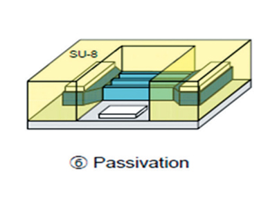
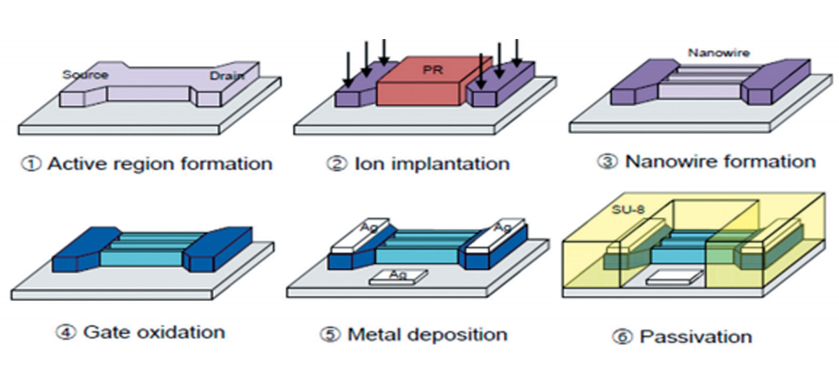
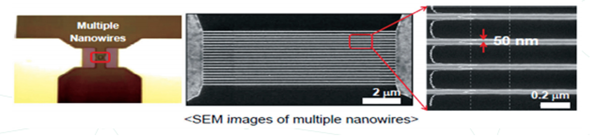
08 BioFET (Silicon Nanowires) 제작 기술
Equipment
- Photo: Stepper ≥ 0.4 μm (5:1 Reticle Lithography)
- Cleaning & Etching: Wet station, Dry Etcher_20 nm, ICP-RIE, DRIE
- Thin Film & Diffusion: E-Beam Evaporator, PE-CVD, Furnace
- Inspection: CD-SEM, FE-SEM, 3D Profiler
Applications
- Electronic detection of DNA
- Protein detection
- Electrical detection of Viruses
Fabrication Result